This is, at long last, part 3 of the overview of my PDP-8/e replica project and offers some details of the low-level implementation.
I have mentioned that I build my PDP-8/e replica from the original schematics. The great thing about the PDP-8/e is that it is still built in discrete logic rather than around a microprocessor, meaning that schematics of the actual CPU logic are available instead of just programmer’s documentation. After all, with so many chips on multiple boards something is bound to break down sooner or later and technicians need schematics to diagnose and fix that1. In addition, there’s a maintenance manual that very helpfully describes the workings of every little part of the CPU with excerpts of the full schematics, but it has some inaccuracies and occasionally outright errors in the excerpts so the schematics are still indispensable.
Originally I wanted to design my own logic and use the schematics as just another reference. Since the front panel is a major part of the project and I want it to visually behave as close as possible to the real thing, I would have to duplicate the cycles exactly and generally work very close to the original design. I decided that at that point I might as well just reimplement the schematics.
However, some things can not be reimplemented exactly in the FPGA, other things are a bad fit and can be improved significantly with slight changes.
Clocks
Back in the day, the rule for digital circuits were multi-phase clocks of varying complexity, and the PDP-8/e is no exception in that regard. A cycle has four timing states of different lengths that each end on a timing pulse.
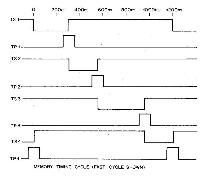
timing diagram from the “pdp8/e & pdp8/m small computer handbook 1972”
As can be seen, the timing states are active when they are at low voltage while the timing pulses are active high. There are plenty of quirks like this which I describe below in the Logic section.
In the PDP-8 the timing generator was implemented as a circular chain of shift registers with parallel outputs. At power on, these registers are reset to all 1 except for 0 in the first two bits. The shift operation is driven by a 20 MHz clock2 and the two zeros then circulate while logic combinations of the parallel outputs generate the timing signals (and also core memory timing, not shown in the diagram above).
What happens with these signals is that the timing states together with control signals decoded from instructions select data outputs and paths while the associated timing pulse combined with timing state and instruction signals trigger D type flip-flops to save these results and present it on their outputs until they are next triggered with different input data.
Relevant for D type flip-flops is the rising edge of their clock input. The length of the pulse does not matter as long as it is not shorter than a required minimum. For example the accumulator register needs to be loaded at TP3 during major state E for a few different instructions. Thus the AC LOAD signal is generated as TP3 and E and (TAD instruction or AND instruction or …) and that signal is used as the clock input for all twelve flip-flops that make up the accumulator register.
However, having flip-flops clocked off timing pulses that are combined with different amounts of logic create differences between sample times which in turn make it hard to push that kind of design to high cycle frequencies. Basically all modern digital circuits are synchronous. There, all flip-flops are clocked directly off the same global clock and get triggered at the same time. Since of course not all flip-flops should get new values at every cycle they have an additional enable input so that the rising clock edge will only register new data when enable is also true3.
Naturally, FPGAs are tailored to this design paradigm. They have (a limited number of) dedicated clock distribution networks set apart from the regular signal routing resources, to provide low skew clock signals across the device. Groups of logic elements get only a very limited set of clock inputs for all their flip-flops. While it is certainly possible to run the same scheme as the original in an FPGA, it would be an inefficient use of resources and very likely make automated timing analysis difficult by requiring lots of manual specification of clock relationships between registers.
So while I do use 20 MHz as the base clock in my timing generator and generate the same signals in my design, I also provide this 20 MHz as the common clock to all logic. Instead of registers triggering on the timing pulse rising edges they get the timing pulses as enables. One difference resulting from that is registers aren’t triggered by the rising edge of a pulse anymore but will trigger on every clock cycle where the pulse is active. The original pulses are two clock cycles long and extend into the following time state so the correct data they picked up on the first cycle would be overwritten by wrong data on the second. I simply shortened the timing pulses to one clock cycle to adapt to this.
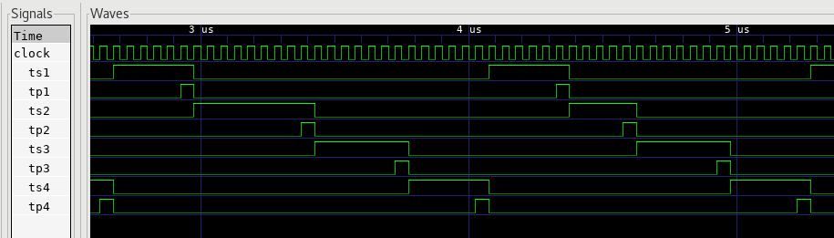
timing signals from simulaton showing long and fast cycle
To reiterate, this is all in the interest of matching the original timing exactly. Analysis by the synthesis tool shows that I could easily push the base clock well over twice the current speed, and that’s already with it assuming that everything has to settle within one clock cycle as I’ve not specified multicycle paths. Meaning I could shorten the timing states to a single cycle4 for an overall more than 10× acceleration on the lowest speed grade of the low-end FPGA I’m using.
Logic
To save on logic, many parts with open collector outputs were used in the PDP-8. Instead of driving high or low voltage to represent zeros and ones, an open collector only drives either low voltage or leaves the line alone. Many outputs can then be simply connected together as they can’t drive conflicting voltages. Return to high voltage in the absence of outputs driving low is accomplished by a resistor to positive supply somewhere on the signal line.
The effect is that the connection of outputs itself forms a logic combination in that the signal is high when none of the gates drive low and it’s low when any number of gates drive low. Combining that with active low signalling, where a low voltage represents active or 1, the result is a logical OR combination of all outputs (called wired OR since no logic gates are involved).
The designers of the PDP-8/e made extensive use of that. The majority of signals are active low, marked with L after their name in the schematics. Some signals don’t have multiple sources and can be active high where it’s more convenient, those are marked with H. And then there are many signals that carry no indication at all and some that miss the indication in the maintenance manual just to make a reimplementer’s life more interesting.
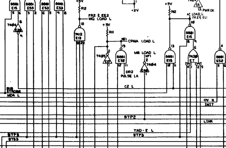
excerpt from the PDP-8/e CPU schematic, generation of the accumulator load (AC LOAD L) signal can be seen on the right
As an example in this schematic, let’s look at AC LOAD L which triggers loading the accumulator register from the major registers bus. It’s a wired OR of two NAND outputs, both in the chip labeled E15, and with pull-up resistor R12 to +5 V. One NAND combines BUS STROBE and C2, the other TP3 and an OR in chip E7 of a bunch of instruction related signals. For comparison, here’s how I implemented it in VHDL:
ac_load <= (bus_strobe and not c2) or
           (TP3 and E and ir_TAD) or
           (TP3 and E and ir_AND) or
           (TP3 and E and ir_DCA) or
           (TP3 and F and ir_OPR);
FPGAs don’t have internal open collector logic5 and any output of a logic gate must be the only one driving a particular line. As a result, all the wired OR must be implemented with explicit ORs. Without the need to have active low logic I consistently use active high everywhere, meaning that the logic in my implementation is mostly inverted compared to the real thing. The deviation of ANDing TP3 with every signal instead of just once with the result of the OR is again due to consistency, I use the “<timing> and <major state> and <instruction signal>” pattern a lot.
One difficulty with wired OR is that it is never quite obvious from a given section of the schematics what all inputs to a given gate are. You may have a signal X being generated on one page of the schematic and a line with signal X as an input to a gate on another page, but that doesn’t mean there isn’t something on yet another page also driving it, or that it isn’t also present on a peripheral port6.
Some of the original logic is needed only for electrical reasons, such as buffers which are logic gates that do not combine multiple inputs but simply repeat their inputs (maybe inverted). Logic gate outputs can only drive so many inputs, so if one signal is widely used it needs buffers. Inverters are commonly used for that in the PDP-8. BUS STROBE above is one example, it is the inverted BUS STROBE L found on the backplane. Another is BTP3 (B for buffered) which is TP3 twice inverted.
Finally, some additional complexity is owed to the fact that the 8/e is made of discrete logic chips and that these have multiple gates in a package, for example the 7401 with four 2-input NAND gates with open collector outputs per chip. In designing the 8/e, logic was sometimes not implemented straightforwardly but as more complicated equivalents if it means unused gates in existing chips could be used rather than adding more chips.
Summary
I have started out saying that I build an exact PDP-8/e replica from the schematics. As I have detailed, that doesn’t involve just taking every gate and its connections from the schematic and writing it down in VHDL. I am changing the things that can not be directly implemented in an FPGA (like wired OR) and leaving out things that are not needed in this environment (such as buffers). Nevertheless, the underlying logic stays the same and as a result my implementation has the exact same timing and behaviour even in corner cases.
Ultimately all this only applies to the CPU and closely associated units (arithmetic and address extension). Moving out to peripheral hardware, the interface to the CPU may be the only part that could be implemented from original schematics. After all, where the magnetic tape drive interface in the original was controlling the actual tape hardware the equivalent in the replica project would be accessing emulated tape storage.
This finally concludes the overview of my project. Its development hasn’t advanced as much as I expected around this time last year since I ended up putting the project aside for a long while. After returning to it, running the MAINDEC test programs revealed a bunch of stuff I forgot to implement or implemented wrong which I had to fix. The optional Extended Arithmetic Element isn’t implemented yet, the Memory Extension & Time Share is now complete pending test failures I need to debug. It is now reaching a state where I consider the design getting ready to be published.
-
There are also test programs that exercise and check every single logic gate to help pinpoint a problem. Naturally they are also extremely helpful with verifying that a replica is in fact working exactly like the real thing. ↩︎
-
Thus 50 ns, one cycle of the 20 MHz clock, is the granularity at which these signals are created. The timing pulses, for example, are 100 ns long. ↩︎
-
This is simply implemented by presenting them their own output by a feedback path when enable is false so that they reload their existing value on the clock edge. ↩︎
-
In fact I would be limited by the speed of the external SRAM I use and its 6 bit wide data connection, requiring two cycles for a 12 bit access. ↩︎
-
The IO pins that interface to the outside world generally have the capability to switch disconnection at run time, allowing open collector and similar signaling. ↩︎
-
Besides the memory and expansion bus, the 8/e CPU also has a special interface to attach the Extended Arithmetic Element. ↩︎