This is an overview of the hardware and internals of the PDP-8/e replica I’m building.
The front panel board
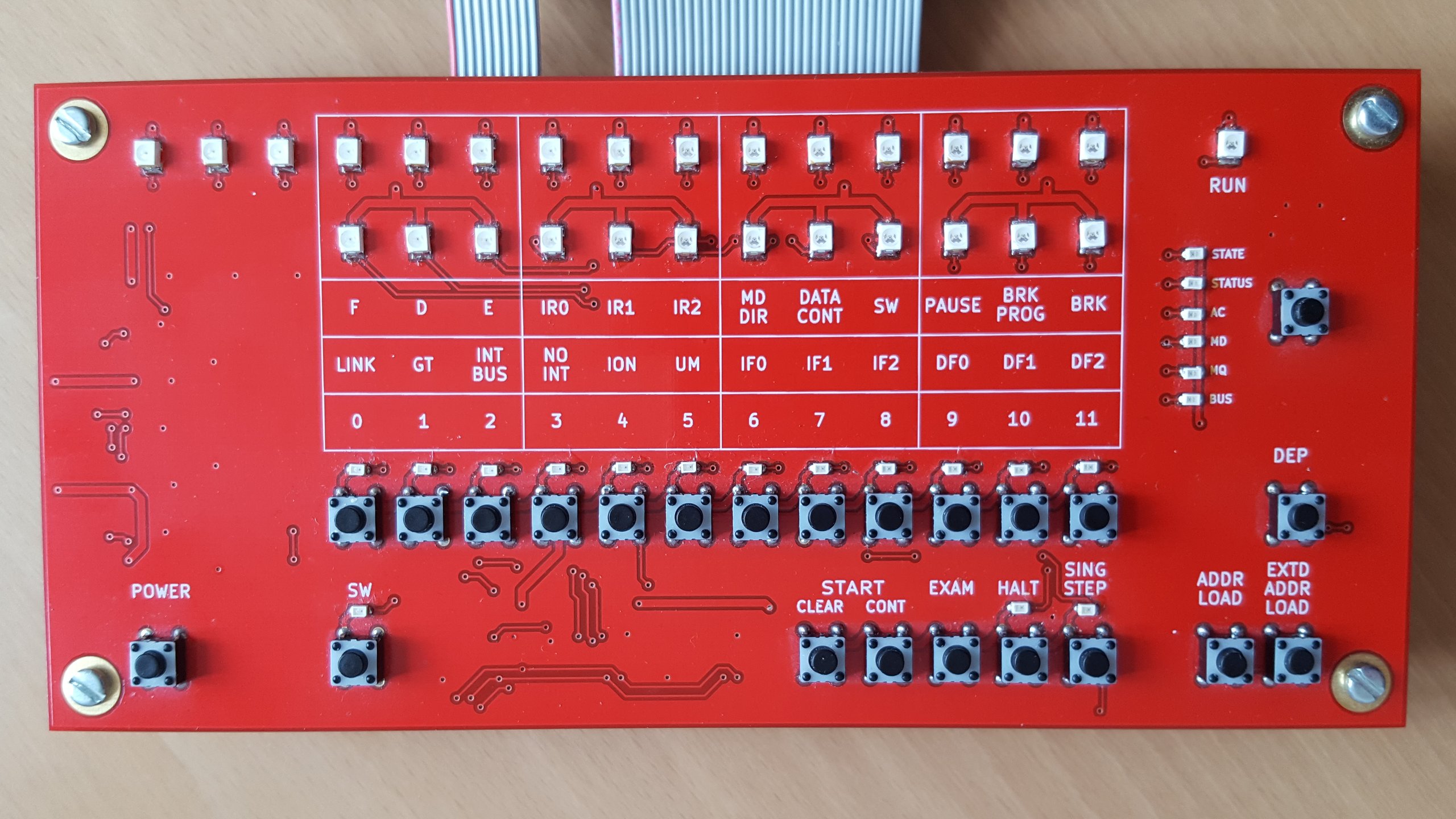
If you know the original or remember the picture from the first post it is clear that this is a functional replica not aiming to be as pretty as those of the other projects I mentioned. I have reordered the switches into two rows to make the board more compact (which also means cheaper) without sacrificing usability.
There’s the two rows of display lights plus one run light the 8/e provides. The upper row is the address made up of 12 bits of memory address and 3 bits of extended memory address or field. Below are the 12 bits indicator which can show one data set out of six as selected by the user.
All the switches of the original are implemented as more compact buttons1. While momentary switches are easily substituted by buttons, all buttons implementing two position switches toggle on/off with each press and they have a LED above that shows the current state. The six position rotary switch is implemented as a button cycling through all indicator displays together with six LEDs which show the active selection.
Markings show the meaning of the indicator and switches as on the original, grouped in threes as the predominant numbering system for the PDPs was octal. The upper line shows the meaning for the state indicator, the middle for the status indicator and bit numbers for the rest. Note that on the PDP-8 and opposite to modern conventions, the most significant bit was numbered 0.
I designed it as a pure front panel board without any PDP-8 simulation parts. The buttons and associated lights are controllable via SPI lines with a 3.3 V supply. The address and indicator lights have a separate common anode configuration with all cathodes individually available on a pin header without any resistors in the path, leaving voltage and current regulation up to the simulation board. This board is actually a few years old from a similar project where I emulated the PDP-8 in software on a microcontroller and the flexible design allowed me to reuse it unchanged.
The main board
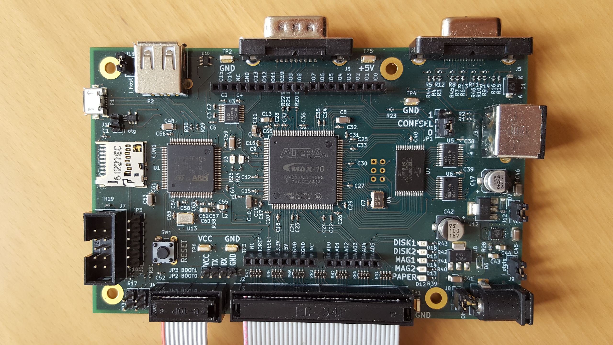
This is where the magic happens. You can see three big ICs on the board: On the left is the STM32F405 microcontroller (with ARM Cortex-M4 core), the bigger one in the middle is the Altera2 MAX 10 FPGA and finally to the right is the SRAM that is large enough to hold all the main memory of the 32 KW maximum expansion of the PDP-8/e. The two smaller chips to the right of that are just buffers that drive the front panel address LEDs, the small chip at the top left is a RS-232 level shifter.
The idea behind this is that the PDP-8 and peripherals that are simple to directly implement, such as GPIO or a serial port, are fully on the FPGA. Other peripherals such as paper and magnetic tape and disks, which are after all not connected to real PDP-8 drives but disk images on a microSD, are implemented on the microcontroller interfacing with stub devices in the FPGA. Compared to implementing everything everything in the FPGA, the STM32F4 has the advantage of useful built in peripherals such as two host/device capable USB ports. 5 V tolerant I/O pins are very useful and simply not available in any FPGA.
I have to admit that this board was a bit of a rush job in order to have something at all to show at the Vintage Computer Festival Europe 18.0. Given that it was my first time designing a board with a large microcontroller and the first time with an FPGA, it wasn’t exactly my fastest progressing project either and I got basic functionality (front panel allows toggling in small programs and running them) working just in time. For various reasons the project hasn’t progressed much since, so the following is still just plans, but plans for which the hardware was designed.
Since the aim is to have a cycle accurate PDP-8/e implementation, digital I/O was always planned. Rather than defining my own header I have included Arduino R3 compatible headers (for 3.3 V compatible boards only) that have become a popular even outside the Arduino world for this purpose. The digital Arduino pins are connected directly to the FPGA and will be directly controllable by PDP-8 software. The downside of choosing the Arduino headers is that the original PDP-8 digital I/O interface is not a perfect match since it naturally has 12 lines whereas the Arduino has 15. The analog inputs are not connected to the FPGA, the documentation of the MAX10’s ADC in the EQFP package are not very encouraging. They are connected to the STM32 instead3.
Another interface connected directly to the FPGA and that would be directly under PDP-8 control is a standard 9 pin RS-232 interface. RX, TX, CTS and RTS are connected and level-shifted between 3.3 V and RS-232 levels by a MAX3232.
Besides the PDP-8, I also plan to implement a full video terminal on the board. The idea is that with a power supply, keyboard and monitor this board would form a complete system without the need of connecting another computer to act as a terminal. To that end, there is a VGA port attached to the FPGA with simple resistor network DACs for 9 bits color (RGB with 3 bits each). This is another spot where I left myself room to expand, for e.g. a VT220 you really only need one color in two brightness levels. Keyboards will be connected either via the PS/2 connector on the right or the USB-A host port at the top left.
Last of the interface ports is the USB micro-AB port on the left, which for now I am using only for power supply. I mainly plan to use it to provide alternative or additional serial ports to the PDP-8 or to export the video terminal serial port for testing purposes. Other possible uses are access to the image files on the microSD and firmware updates.
This has gotten rather long again, so I’m stopping here and leave some implementation notes for another post.
-
They are also much cheaper. Given the large number of switches, the savings are substantial. Additionaly the buttons are nicer to operate than long rows of tiny switches. ↩︎
-
Or rather Intel now. At least Altera’s web site, documentation and software have already been thoroughly rebranded, but the chips I got were produced prior to that. ↩︎
-
That’s not to say that the analog conversions on the STM32 are necessarily better than those of the MAX10 when you can’t follow their guidelines, I have no comparisons. Certainly following the guidelines would have been prohibitive given how many pins’ usage they restrict. ↩︎